Process files and extraction
EMIR keeps every process number in one YAML file per PDK, the process file
(--process); no limit lives in the code. This page says where the files come from, how
to write one (from the PDK's files, an ICT, or typed by hand from the design manual),
every key, what the extracted DSPF must contain, and how magic extracts one on SKY130.
Screening, not sign-off. A process file is a reading of the PDK's data, not the foundry's qualified rule deck.
A minimal file
pdk: my_pdk (from the tech LEF, rev X)
em_tref: 105.0                  # C, where the LEF quotes its limits
temp_reference: 25.0
layers:
  M1:
    gds: [10, 0]
    sheet_res: 0.08             # ohm/sq at 25 C
    tc1: 0.0035
    min_width: 0.1
    jmax_avg: 1.5               # mA/um at 105 C
  M2:
    gds: [12, 0]
    sheet_res: 0.08
    tc1: 0.0035
    min_width: 0.1
    jmax_avg: 1.5
vias:
  V1:
    gds: [11, 0]
    below: M1
    above: M2
    res: 4.0                    # ohm per cut
    vcwidth: 0.1                # um
    imax_avg: 0.2               # mA per cut
(The numbers are invented; a real file cites a source for each.) Units: lengths in
um, resistance in ohm (per square for wires, per cut for vias), limits in mA per um of
drawn width for wires and mA per cut for vias, temperatures in C.
emir schema process prints the JSON Schema; pdks/TEMPLATE.yaml has every
key with comments.
The files in pdks/
| file | PDK | metal stack | limits quoted at |
|---|---|---|---|
sky130.yaml |
SkyWater SKY130 (sky130A) |
li1, met1 to met5; mcon, via, via2 to via4; and the magic: section |
90 C |
gf180mcu.yaml |
GlobalFoundries GF180MCU (gf180mcuD) |
Metal1 to Metal5; Via1 to Via4 | 125 C |
ihp_sg13g2.yaml |
IHP SG13G2 | Metal1 to Metal5, TopMetal1 and 2; their vias | 105 C |
They are built only from the PDKs' own public files (Apache-2.0, the open PDKs' licences),
and every value names its source as [FILE]:line. With the PDKs installed,
pytest tests/test_pdks.py -k citations checks every cited line still holds its value.
pdks/README.md lists what each PDK does not publish (no peak limits
on any of the three, no rms limits on vias): those metrics are reported as not checked.
Writing one for your PDK
- Copy
pdks/TEMPLATE.yamland changepdk:(a name containing "illustrative" warns that the limits are not real,EMIR-W306). - Fill each conductor layer from the PDK's documents: sheet resistance at
temp_reference, the TCRs, and the EM limits in mA/um at the temperature inem_tref. Fill each via:below,above, ohm per cut, the cut sidevcwidth, the limits in mA per cut. Cite each value in a comment. - Leave out what the PDK does not publish: a missing limit is reported as not checked. Never estimate one.
- Map the extractor's layer names that do not match with
dspf_layers(m1_conn_a: Metal1, or1: Metal1for a$lvl=1level number). - Check it:
emir check --process my_pdk.yamlalone, thenemir check <dspf> --process my_pdk.yaml, and one hand-checkable wire at its limit (sky130's met1 allows 2.8 mA/um: a 0.14 um wire may carry 0.392 mA;tests/test_pdks.pyruns that strap).
From a foundry ICT: emir import-ict --ict <pdk>.ict --emir my_pdk.yaml -o new.yaml
fills the EM limits, TCRs, jmax_factor and em_tref onto the geometry already in the
file. A J x (w - dw) limit becomes J with width_loss_um: dw; the long-wire branch
is taken (the conservative one); a via rms or peak limit the ICT does not give is not
written. A file made from a licensed PDK's data stays with that PDK installation, never
in this repository (the leak guard refuses ICT, tech-file and layer-map files).
Unit traps: a density per cross-section (MA/cm^2) is not mA/um (multiply by the
metal thickness: 1 MA/cm^2 = 10 mA/um^2); a via limit or resistance per array is not per
cut; vcwidth is the cut's side, not its area; em_tref (where the limits hold) is not
temp_reference (where the sheet resistance holds); a LEF's fixed rms limit is
jmax_rms, an ICT's self-heating constant jmax_rms_k, never both (EMIR-E310); give
the unidirectional DC average limit, not a bidirectional one. emir check flags a value
outside its quantity's plausible range (EMIR-W321: an A-for-mA or nm-for-um slip), but
not a factor of ten.
Entering EM data by hand
When no readable process data exists (not in pdks/, and no ICT, or an encrypted one:
emir import-ict refuses it, EMIR-E325, and never tries to decrypt it), the person
types the EM data from the design manual:
emir process new --from-dspf block.dspf -o my_pdk.yaml     # the fill-in file
emir process check my_pdk.yaml --dspf block.dspf            # what is still missing
- The fill-in file covers exactly the layers and vias the DSPF uses, every value
nullwith its unit and asources:slot, the via stacking it inferred marked to be checked, andprovenance: hand-entered. It never overwrites a file (EMIR-E326). - Type each value as the manual prints it, with its source (
sources: {jmax_avg: "DM
  rev 2.1, table 9-4, p. 112"}
); leave null what the manual does not give. At a terminal,emir process new ... --interactiveasks for each value; an agent never drives it (EMIR-E327). - The check lists what is still empty (
EMIR-E320for a required value), without a source (EMIR-W320), unconfirmed stacking (EMIR-W324), likely unit slips (EMIR-W321) and limits out of order (EMIR-W322). A likely slip on a temperature, the derating or a limit blocks the run (EMIR-E331) until it is corrected or the person lists its path underunit_confirmed:. It must pass before any run. - Every report says per layer that the limits were typed by hand, and from which
document (
limits_provenance).
Two forms the manuals print are read as printed. A width loss, I_max = J x (W -
dW), is width_loss_um: dW (for J = 2.0 mA/um and dW = 0.02 um, a 0.30 um wire may carry
0.56 mA, 7 % stricter than 0.60 mA; a wire no wider than dW is refused, EMIR-E323).
Black's equation, MTTF = A J^-n exp(Ea / (k T)), is derating: {model: black,
ea_eV: Ea, n: n}: the avg limits scale by exp[(Ea / (n k)) (1/T - 1/Tref)] (Ea = 0.9 eV,
n = 2, from 105 C to 125 C: x0.4997); below em_tref they are held as quoted
(EMIR-W326). emir validate holds both to a closed form.
Top level
| key | required | meaning |
|---|---|---|
pdk |
no | the name reports show; its first word is the PDK's directory under $PDK_ROOT (magic's startup file) |
provenance |
no | hand-entered, imported-ict, public-pdk-data or mixed: reports say it per layer; a hand-entered value with no source gets EMIR-W320 |
sources |
no | where em_tref, temp_reference, jmax_factor and derating came from |
em_tref |
yes | C, the temperature the average limits hold at, and the default analysis temperature (no default: EMIR-E312) |
temp_reference |
no | C, where sheet_res holds (default 25) |
warn_fraction |
no | the ratio from which an item is WARN (default 0.8) |
jmax_factor |
no | {C: factor}, the derating of the average limits, 1.0 at em_tref |
derating |
no | {model: black, ea_eV, n}, Black's equation; give it or jmax_factor, never both (EMIR-E321) |
unit_confirmed |
no | paths of values outside their usual range that the person checked against the manual |
dspf_layers |
no | {token or $lvl number: name}, for extractor names that do not match |
magic |
no | the magic route (below) |
layers |
yes | the conductor layers (at least one) |
vias |
no | the cut layers |
ict_conductor_pattern |
no | emir import-ict: the ICT block name for a layer (default {layer}_conn) |
ict_process |
no | written by emir import-ict, for the record |
An unknown key inside a layer or via is a FAIL (EMIR-E316: a misspelt limit would go
unchecked); an unknown top-level key warns (EMIR-W314). Any value may be null: a
limit left empty is not checked, a required value left empty is a FAIL (EMIR-E320).
A conductor layer
| key | unit | meaning |
|---|---|---|
gds |
[layer, datatype] | for the person; no path reads it |
sheet_res |
ohm/square | at temp_reference (required) |
tc1 |
1/C | the linear TCR: R(T) = R (1 + tc1 dT + tc2 dT^2), dT from temp_reference |
tc2 |
1/C^2 | the quadratic TCR |
min_width |
um | the PDK's rule, for the record |
jmax_avg |
mA/um | the DC average limit at em_tref, derated at other temperatures |
jmax_rms |
mA/um | a fixed rms limit, as a tech LEF gives it |
jmax_rms_k |
(mA/um)^2 per C | an ICT's self-heating form: the limit is sqrt(jmax_rms_k x delta_T) |
jmax_peak |
mA/um | the peak limit |
width_loss_um |
um | the dW of I_max = J x (W - dW) |
sources |
where each value came from | |
provenance |
this entry's own, in a mixed file |
|
estimate |
true flags the limits as estimates in every report | |
ict_name |
emir import-ict: this layer's ICT block |
A via
| key | unit | meaning |
|---|---|---|
gds |
[layer, datatype] | the cut layer |
below |
the conductor under the cut (required) | |
above |
the conductor over the cut (required) | |
res |
ohm per cut | required; not scaled with temperature |
vcwidth |
um | the cut's side: turns an extracted cut area ($A) into a count. Without it such a via is checked as one cut (EMIR-W308) |
imax_avg |
mA per cut | the DC average limit at em_tref, derated at other temperatures |
imax_rms |
mA per cut | the rms limit |
imax_peak |
mA per cut | the peak limit |
estimate |
flags the average limit as an estimate | |
rms_peak_estimate |
flags imax_rms and imax_peak as estimates: they are not applied |
|
sources |
as for a layer | |
provenance |
as for a layer | |
ict_name |
emir import-ict: the ICT via block |
The magic section
| key | meaning |
|---|---|
binary |
the magic to try, a magic program's bare name on $PATH (a path is refused, EMIR-E648) |
layers |
magic's layer names onto the file's (locali: li1, viali: mcon on sky130) |
devices |
each device model's terminal names in magic's order ("sky130_fd_pr__nfet_*": [d, g, s, b]); others get t1, t2 ... (EMIR-W643) |
sources |
where the values came from |
--process FILE wins; then $EMIR_PROCESS; then the site file's process:
($EMIR_SITE, else ~/.emir/site.yaml, never committed).
The DSPF
EM needs each wire's width (J = I / W) and each via's cut count: SPEF has no
geometry, a DSPF with geometry annotation does. emir check <dspf> --process <file>
names every gap before anything is computed.
| record | what EMIR takes from it |
|---|---|
| *|OPERATING_TEMPERATURE | the extraction temperature (resistance is scaled to the analysis temperature) |
| *|NET, *|P | the net, and the port where it is fed (the IR reference) |
| *|I (node inst pin dir cap x y) | where a device pin lands: simulated currents attach here (without x y the record is dropped) |
| *|S (node x y) | sub-node coordinates, for the maps |
R... n1 n2 value $layer $W= $L= ... |
a wire: its layer and drawn width ($W or $SI_W); without a width, a FAIL (EMIR-E210) |
R... $cont $N= / $VC= / $A= |
a via: its cut count, or its cut area turned into a count with vcwidth |
Extraction settings, whatever the extractor: no series reduction (one resistor per
drawn segment, so a neck is not averaged away), width and layer on every wire, a cut
count or area on every via, node and instance-pin coordinates, the extraction
temperature stated, ideally the EM analysis temperature.
Quantus: Cadence; Calibre and StarRC: notes in agent/cadence/
(UNVERIFIED). An R-only netlist is not the netlist to simulate: it has no capacitance.
| currents | the DSPF EMIR screens | the netlist you simulate |
|---|---|---|
| a simulation (rcc) | the RC extraction | the same RC extraction, every resistor current saved |
DC (--currents) |
R-only or RC | none |
SKY130: magic extracts the DSPF
On SKY130, with a GDS and no DSPF, magic extracts one: emir extract --tool magic has
magic keep every resistor as one drawn segment, with its layer, width, length and place,
and writes the DSPF.
emir next --gds blk.gds --process pdks/sky130.yaml --cell blk --format json
emir extract --tool magic --gds blk.gds --cell blk --process pdks/sky130.yaml --out emir_out/extract_blk
emir next --dspf emir_out/extract_blk/blk.dspf --process pdks/sky130.yaml --netlist tb.cir \
    --gds blk.gds --cell blk --format json
<out>/<cell>.dspf is the network, and the RC netlist an rcc testbench includes. From
there the flow is the one on
Simulators. With --html, emir run --gds blk.gds --cell blk draws the
layout under the chart.
The magic it needs. A stock magic writes each resistor's value only. The geoout
patch adds extresist geoout on, which writes each resistor's layer, direction, width,
length and end points (<cell>.res.geo). It is public: branch
extresist-geoout of
codervijay/magic, offered upstream as
RTimothyEdwards/magic#562 (open).
git clone -b extresist-geoout https://github.com/codervijay/magic magic-geo
cd magic-geo && ./configure --prefix=$HOME/magic-geo && make && make install
export EMIR_MAGIC=$HOME/magic-geo/bin/magic
EMIR tries --magic, $EMIR_MAGIC, the process file's magic: binary:, the site file's
magic:, then magic-8.3.515-geo and magic on $PATH, and uses the first that answers
extresist geoout; with none it exits 3 (EMIR-E643) and says how to build one. The
examples were made with magic 8.3.515 and the patch (the branch is on 8.3.684; the test
cells in tests/data/magic_tiny give the same resistor network with both). magic's
technology is $PDK_ROOT/<pdk>/libs.tech/magic/<pdk>.magicrc (--magicrc overrides it).
What it writes. The cell is flattened first (a hierarchical layout extracts as the
flat one would). Every conductor magic extracts is in the network (contacts, local
interconnect, diffusion, poly, wells); a layer with no limit carries its current in the
IR drop and is reported as not checked (on sky130: li1 and below). Each device terminal
is a *|I record named from magic: devices:. A port drawn with several pins gets a
node per pin, tied to the port by 0 V sources (--port-pins tied, the default), so every
pin is fed. Capacitors are counted once. The DSPF writer and the geometry reader are
ported from the Skycadeda Analog Framework (SAF), with credit and the licence in
THIRD_PARTY_NOTICES.md.
Example 08. examples/08_open_layout runs the route on a
synthetic SKY130 cell: four two-finger NMOS whose out and vss each reach their pad
through one via2 cut. magic extracted 1135 resistors; the gate is pulsed, Xyce 7.10, 90 C:
| run | out: IR, worst ratio | vss: IR, worst ratio |
|---|---|---|
| rcc | 6.6910 mV, 1.3566x (via2: 1 -> 2 cuts) | 4.8448 mV, 1.3566x |
rcc's 440 checked branches equal the simulator's own currents to 7.8e-13, and its IR the simulator's own node voltages to 3.2e-7.
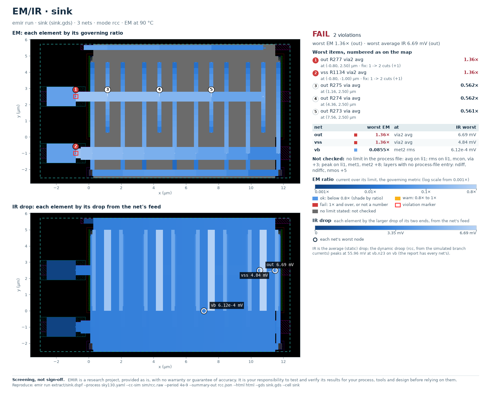
Example 08: the chart of its rcc run (synthetic layout, the SKY130 limits of pdks/sky130.yaml).
Limits of the route: it needs the patched magic until the patch is in a magic release;
tested on sky130 only (gf180mcu and IHP SG13G2 not tried), on small cells; a wire on a
diagonal shape is checked at magic's tile extent and listed as not checked
(EMIR-W647); a net magic leaves whole has nothing to check (EMIR-W645); label every
net.